Mingxing Li 1,2Yueke Wang 1,2,4,*Tian Sang 1,2,5,*Hongchen Chu 3,6,*[ ... ]Guofeng Yang 1,2
Author Affiliations
Abstract
1 Optical Information Science and Technology Department, Jiangnan University, Wuxi 214122, China
2 Optoelectronic Engineering and Technology Research Center, Jiangnan University, Wuxi 214122, China
3 National Laboratory of Solid State Microstructures, School of Physics, and Collaborative Innovation Center of Advanced Microstructures, Nanjing University, Nanjing 210093, China
4 e-mail: ykwang@jiangnan.edu.cn
5 e-mail: sangt@jiangnan.edu.cn
6 e-mail: chuhongchen@nju.edu.cn
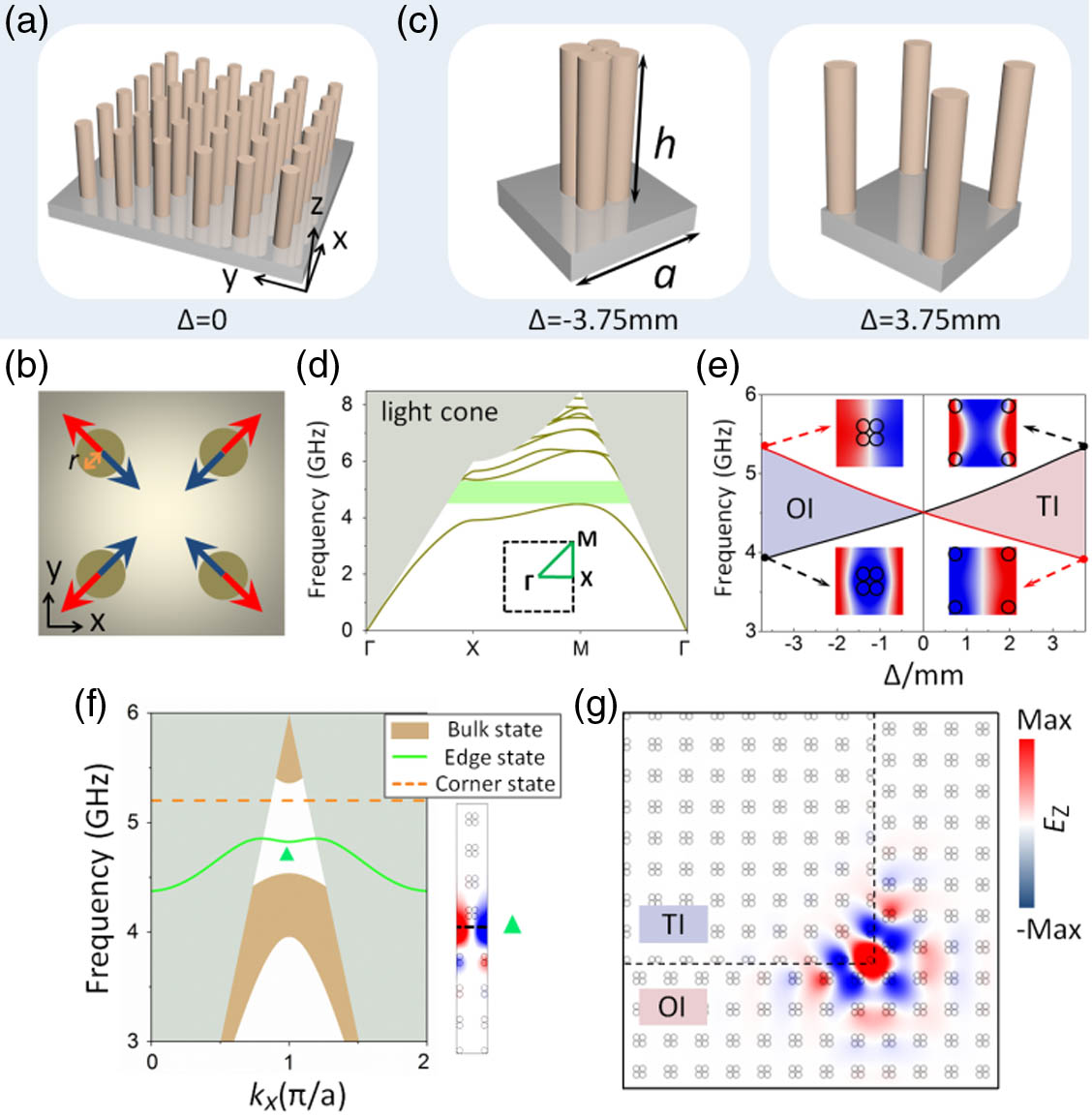
The photonic topological insulator has become an important research topic with a wide range of applications. Especially the higher-order topological insulator, which possesses gapped edge states and corner or hinge states in the gap, provides a new scheme for the control of light in a hierarchy of dimensions. In this paper, we propose a heterostructure composed of ordinary-topological-ordinary (OTO) photonic crystal slabs. Two coupled edge states (CESs) are generated due to the coupling between the topological edge states of the ordinary-topological interfaces, which opens up an effective way for high-capacity photonic transport. In addition, we obtain a new band gap between the CESs, and the two kinds of coupled corner states (CCSs) appear in the OTO bend structure. In addition, the topological corner state is also found, which arises from the filling anomaly of a lattice. Compared with the previous topological photonic crystal based on C-4 lattice, CESs, CCSs, and the topological corner state are all directly observed in experiment by using the near-field scanning technique, which makes the manipulation of the electromagnetic wave more flexible. We also verify that the three corner states are all robust to defects. Our work opens up a new way for guiding and trapping the light flow and provides a useful case for the coupling of topological photonic states.
Photonics Research
2022, 10(1): 01000197
光子学报
2021, 50(11): 1123002

Author Affiliations
Abstract
1 School of Science, Jiangsu Provincial Research Center of Light Industrial Optoelectronic Engineering and Technology, Jiangnan University, Wuxi 214122, China
2 School of Electronic and Information Engineering, Changshu Institute of Technology, Changshu 215556, China
3 The 38th Research Institute of China Electronics Technology Group Corporation, Hefei 230000, China
We have fabricated the AlGaN solar-blind ultraviolet metal–semiconductor–metal (MSM) photodetectors (PDs) with an Al composition of 0.55. The surface roughness and dislocations of the high-Al-content epitaxial layer are analyzed by atomic force microscopy and transmission electron microscopy, respectively. The device exhibits high spectral responsivity and external quantum efficiency due to the photoconductive gain effect. The current reveals a strong dependence on high temperatures in the range of 4–10 V. Moreover, the Poole–Frenkel emission model and changing space charge regions are employed to explain the carrier transport and photoconductive gain mechanisms for the AlGaN PD, respectively.
metal–semiconductor–metal solar blindness photodetector Poole–Frenkel emission photoconductive gain Chinese Optics Letters
2021, 19(8): 082504
1 江南大学理学院, 江苏 无锡 214122
2 国家超级计算无锡中心, 江苏 无锡 214100
3 江苏省轻工光电工程技术研究中心, 江苏 无锡 214122
4 江苏省模式识别与智能计算工程实验室, 江苏 无锡 214100
为了准确预测反射型半导体光放大器(RSOA)中的放大自发辐射(ASE)噪声和掌握RSOA的最佳工作区间, 在SOA宽带稳态模型以及高效动态模型的基础上, 修改了RSOA的部分结构并将多阶迭代的算法运用到RSOA理论建模以及增益噪声指数测试中。实验结果表明RSOA在偏置电流大于130 mA时增益稳定在26 dB以上, 噪声指数稳定在11 dB。且在偏置电流不变时, 低输入功率-30 dBm时, RSOA处于最佳工作区间。该种新型RSOA模型满足且优于实际应用中RSOA的各项工作参数, 测试结果对RSOA的产品优化设计和光网络单元最佳工作区间具有指导和改进的意义。、
光通信 反射型半导体放大器 多阶迭代算法 增益特性 噪声指数 optical communication RSOA multi-order iterative algorithm gain characteristics noise figure

Author Affiliations
Abstract
1 School of Science, Jiangsu Provincial Research Center of Light Industrial Optoelectronic Engineering and Technology,Jiangnan University, Wuxi 214122, China
2 School of Electronic Science and Engineering, Nanjing University, Nanjing 210093, China
Monolithic white-light-emitting diodes (white LEDs) without phosphors are demonstrated using InGaN/GaN multiple quantum wells (MQWs) grown on GaN microrings formed by selective area epitaxy on SiO2 mask patterns. The microring structure is composed of {1-101} semi-polar facets and a (0001) c-plane, attributed to favorable surface polarity and surface energy. The white light is realized by combining short and long wavelengths of electroluminescence emissions from InGaN/GaN MQWs on the {1-101} semi-polar facets and the (0001) c-plane, respectively. The change in the emission wavelengths from each microfacet is due to the In composition variations of the MQWs. These results suggest that white emission can possibly be obtained without using phosphors by combining emission light from microstructures.
Light-emitting diodes Light-emitting diodes Quantum-well Quantum-well -wire and -dot devices -wire and -dot devices Photonics Research
2016, 4(1): 01000017
西安工业大学 光电工程学院, 陕西 西安710021
根据光学系统的装校工艺过程, 应用开发工具Delphi, 研制了用于光学系统装校的光学系统中心偏误差分析软件。该软件提供了光学元件球心像位置计算和光学中心偏误差分析的功能, 人机界面友好、操作简单方便, 目前已经较好地应用于高精度光学中心偏测量仪的光学装校工艺过程的控制。
光学中心偏 球心像 误差分析 optical decentration central image error analysis
西安工业大学 光电工程学院, 陕西 西安 710021
分析激光打标工艺参数对不同颜色基底ABS材料激光打标效果和质量的影响。采用Nd∶YAG1064 nm端泵激光打标设备,使用不同功率、频率、焦距等参数,分别对白、粉、红、蓝和黑5种基底颜色的丙烯腈-丁二烯-苯乙烯共聚物(ABS)塑料进行红外激光打标,并对打标后材料的微观结构进行了表征。结果表明,不同颜色的ABS材料的打标性能各不相同,ABS材料的基底颜色对激光打标效果影响较大。实验获得了不同基底颜色ABS材料激光打标的工艺参数,为进一步研究提供借鉴。
激光打标 评价方法 工艺参数 laser marking ABS ABS evaluating method technical parameters
Author Affiliations
Abstract
1 Key Laboratory of Advanced Process Control for Light Industry (Ministry of Education), Department of Electronic Engineering, Jiangnan University, Wuxi 214122, Jiangsu, China
2 The 38th Research Institute of China Electronics Technology Group Corporation, Hefei 230088, China
We study the performance of GaN-based p–i–n ultraviolet (UV) photodetectors (PDs) with a 60 nm thin p-type contact layer grown on patterned sapphire substrate (PSS). The PDs on PSS exhibit a low dark current of ~2 pA under a bias of -5 V, a large UV/visible rejection ratio of ~7×10³, and a high-quantum efficiency of ~40% at 365 nm under zero bias. The average quantum efficiency of the PDs still remains above 20% in the deep-UV region from 280 to 360 nm. In addition, the noise characteristics of the PDs are also discussed, and the corresponding specific detectivities limited by the thermal noise and the low-frequency 1/f noise are calculated.
230.0250 Optoelectronics 230.5160 Photodetectors 230.5440 Polarization-selective devices Chinese Optics Letters
2014, 12(9): 092301
设计了InGaN/GaN 超晶格垒层替代p-GaN 和n-GaN 附近传统GaN 垒层的InGaN/GaN 多量子阱(MQW)发光二极管(LEDs)结构。通过数值方法模拟出两种LED 结构的光功率-电压(L-V)曲线、电致发光(EL)谱、能带图、电子浓度分布和辐射复合速率。结果表明InGaN/GaN 超晶格替代n-GaN 附近GaN 垒层的LED 结构比替代p-GaN 附近GaN 垒层的LED 显示出更高的发光强度。这种发光增强的原因是InGaN/GaN 超晶格替代n-GaN 附近GaN 垒层可以提高电子注入效率和辐射复合速率。
发光二极管 超晶格垒层 数值模拟 激光与光电子学进展
2014, 51(3): 032301
利用选择性横向外延技术生长{11-22}半极性面GaN模板,并利用半极性面模板生长InGaN/GaN多量子阱结构。结果表明,生长出的GaN模板由半极性面{11-22}面和c面组成,多量子阱具有390 nm和420 nm的双峰发光特性,局域阴极发光(CL)测试表明390 nm附近的发光峰来源于半极性面上的量子阱发光,而420 nm左右的发光峰源于c面量子阱发光。c面量子阱发光相对于斜面量子阱发光发生显著红移是因为在选择性横向外延生长过程中,In组分相比Ga较易从掩模区域向窗口中心区域迁移,形成了中心高In组分的c面量子阱,而半极性面上InGaN/GaN多量子阱量子限制斯塔克效应相比于极性面会减弱,此外,相同生长条件下半极性面的生长速率低于极性c面的生长速率。
光学器件 选择性横向外延 GaN半极性面 多量子阱 极化效应 激光与光电子学进展
2014, 51(2): 022302


